We present an extensive study on electrical spectroscopy of graphene ribbons and edges of highly oriented pyrolytic graphite (HOPG) using atomic force microscope (AFM). We have addressed in the present study two main issues (1) How does the electrical property of the graphite (graphene) sheet change when the graphite layer is displaced by shear forces? And (2) How does the electrical property of the graphite sheet change across a step edge? While addressing these two issues we observed (1) variation of conductance among the graphite ribbons on the surface of HOPG. The top layer always exhibits more conductance than the lower layers, (2) two different monolayer ribbons on the same sheet of graphite shows different conductance, (3) certain ribbon/sheet edges show sharp rise in current, (4) certain ribbons/sheets on the same edge shows both presence and absence of the sharp rise in the current, and (5) some lower layers at the interface near a step edge shows a strange dip in the current/conductance. We discuss possible reasons for such rich conducting landscape on the surface of graphite.
Extensive theoretical and experimental studies have been made on layered graphite material to understand its complex electrical behavior. Recently, electronic properties of graphene nanostructures, such as carbon nanotubes, carbon nanocones, fullerenes, and graphite edges, have attracted much attention from the point of view of basic research and applications. The motivation for studying carbon based nanostructures is to develop atomic or molecular nanometer scale electronic devices having a fundamentally different operating principle than conventional electronic devices. Due to its nanoscale size one can look at opportunities to increase the device density as well. The electronic property of nanoscale materials are strongly influenced by their geometries. The graphene sheets are generally self-assembled to arrive at various shaped nanoobjects such as carbon single-walled and multiwalled nanotubes, fullerenes, nanocones, etc.,. The electronic properties of these objects strongly depend on the manner in which these graphene sheets are cut and joined at the edges. Any new information and understanding related to graphene sheets will have an impact on basic research and applications of carbon based materials.

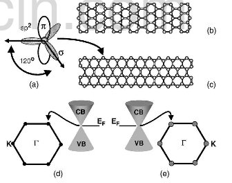
Fig.1-(a)carbon atoms (b)graphite sheet,ribbons (c)zigzag edge (d) six point in the brillouin zone (e) finite overlap of CB VB
HOPG is a periodical stack of 2D graphene sheets/ layers along the c axis. Each sheet is comprised of hexagonal lattice of carbon bonded by strong σ bonding in the a-b plane. See Fig.1 (a). The perpendicular π–orbital electrons are responsible for the conductivity along the a-b plane. The conduction occurs by the quantum mechanical hopping of these electrons. Each of these layers are weakly bonded to their neighboring layers by interlayer interaction forces. Because of the weak interlayers interaction forces, the graphene layers can easily slide against each other and peel off easily. In late 1950s and early 1960s the electronic property of graphite was evaluated using phenomenological models based on the symmetry of graphite. The dispersion relation of the bands was found to have a very slight overlap of the valence and conduction bands at the Fermi level, where the electron density is very low. This causes graphite to have semimetallic characteristics. Even though the change carrier concentration is very low, the electrical mobility of these carriers is high and its electrical resistivity along the plane is -40 μΩcm. The temperature coefficient of resistivity of HOPG is positive along the sheet and ρ⊥/ρ∥≈104at room temperature.
It has been pointed out the graphene sheet edges strongly affect the π electronic states. The edges of the graphene sheets are of two types (1) armchair and (2) zigzag edges. These two edges are shown in Fig.1 (b) and (c), respectively. It was shown theoretically that graphene sheets having zigzag edges possess edge states localized at the zigzag edges. In contrast, armchair edges have no edge states at its edges, hence making the armchair edge less conducting than the zigzag edge.